
NEW DELHI, November 7: India has opened applications for the second phase of its semiconductor programme and approved 12 more electronics component projects, Electronics and IT Minister Ashwini Vaishnaw announced on Friday. The Semicon 2.0 web portal now accepts applications for chip-making machines and materials, new fabs and chip assembly and testing units, while the 12 new component projects bring projected investment of ₹7,503 crore.
Key highlights
- Semicon 2.0 portal: applications are open for Pillar 2 (machines and materials), Pillar 3 (more fabs) and Pillar 4 (chip assembly and testing, or ATMP/OSAT).
- Outlay: the Cabinet has approved Semicon 2.0 with ₹1,27,500 crore under the India Semiconductor Mission.
- Phase one: 12 chip projects approved across six states with over ₹1.64 lakh crore of investment; five had started commercial production by October 2026.
- New component approvals: 12 projects worth ₹7,503 crore, with projected production of ₹39,045 crore and 7,127 direct jobs.
- Firsts: the first approvals under the component scheme for copper foil, cathode active material and specialty ceramics.
| Product | Company |
|---|---|
| Multi-layer printed circuit boards | NeST ICELR Pvt Ltd |
| Relays | TDConnex (Chennai) Pvt Ltd |
| Heat sinks | Modern Automotives Ltd |
| Specialty ceramics | Voltix Semicon Pvt Ltd |
| Copper foil | Indo Asia Copper Ltd |
| Anode material for lithium-ion cells | TACC Ltd |
| Cathode active material | Vidyuta Materials Pvt Ltd |
| Polypropylene film (capacitor grade) | Enerfolie LLP |
| Camera rims | Surface Modification Technologies Pvt Ltd |
| Precision moulds and tooling | TDConnex (Chennai) Pvt Ltd |
| Power and control systems for capital equipment | Rockwell Automation India Pvt Ltd |
| Factory automation equipment and system integration | Wipro Pari Robotics Pvt Ltd |
What Semicon 2.0 covers
Semicon 2.0 has six pillars: chip design, machines and materials, more fabs, assembly and testing, research and development, and talent. Mr Vaishnaw said the new phase would focus on equipment, materials, chemicals and gases, with a target of bringing at least three major equipment makers and five chemicals and gases companies to India. He said quality, technological depth, R&D and global competitiveness must guide project selection.
The ministry said the first phase also gave 105 start-ups access to chip-design (EDA) software, funded 24 start-ups, and provided EDA tools to 332 institutions under the Chips to Startup programme, which has trained about 70,000 students.
The component scheme so far
The new projects are spread across seven states: Gujarat, Karnataka, Madhya Pradesh, Maharashtra, Punjab, Tamil Nadu and Uttar Pradesh. Mr Vaishnaw said nearly half of the units approved under the scheme are small and medium enterprises. With this round, the Electronics Components Manufacturing Scheme (ECMS) has approved 118 applications covering 34 products in 16 states, with expected investment of ₹77,051 crore, projected production of ₹5,73,146 crore and 81,755 direct jobs.
Our calculation
- The average new project brings about ₹625 crore of investment.
- For this batch, projected production is about 5.2 times the investment; for the scheme as a whole it is about 7.4 times.
- This round adds about 9.7% to the scheme’s total expected investment.
- The new projects promise about 95 direct jobs for every ₹100 crore invested.
What it means for India and Asia
Most of the materials in this round, such as copper foil, battery cathode and anode materials and capacitor film, sit deep in the supply chain for phones, servers and electric vehicles, and India has relied on imports for them. Making them at home is part of India’s bid to win a larger share of electronics manufacturing that is now concentrated in East and South-East Asia. The test will be how many of the approved projects reach production on time; five of the 12 first-phase chip projects are already producing.
What to watch
- Which companies apply for fabs and equipment projects under Semicon 2.0.
- Whether major global equipment and chemicals suppliers commit to Indian plants.
- Production start dates for the newly approved component units.
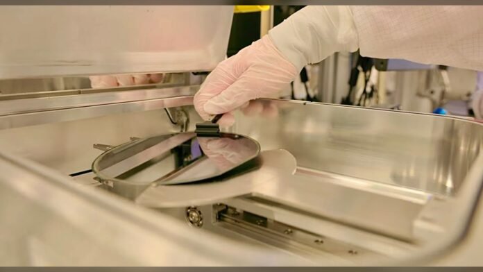
A semiconductor wafer being removed from processing equipment (representative image). Image: Purdue Engineering, CC BY 4.0, via Wikimedia Commons. Photo source · Licence
Sources

The Business Desk covers markets, the economy, companies and personal finance. Stories are checked against at least two credible sources before publication.